digitaal/analoog converter


digitaal/analoog converter
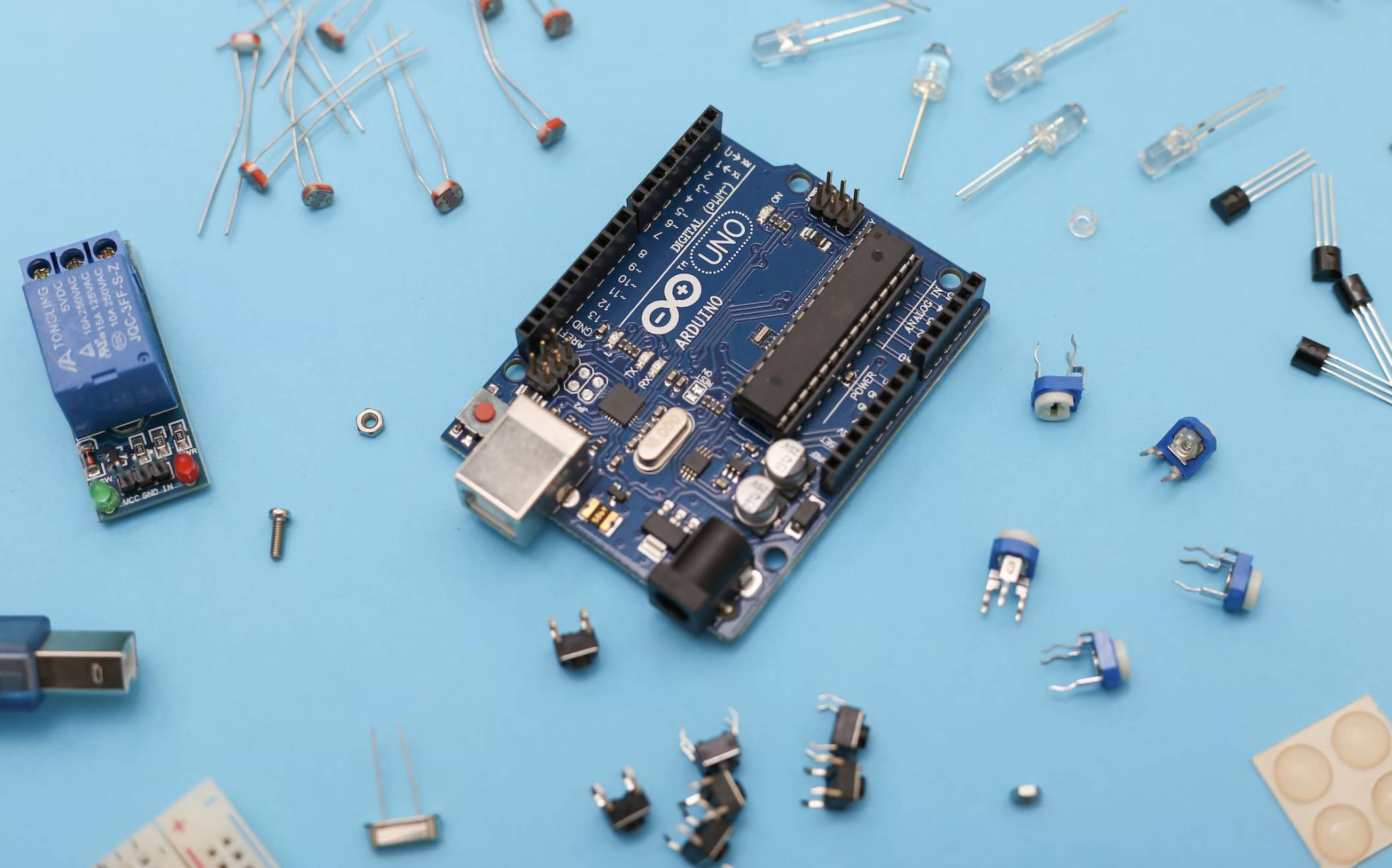
A PCF8591 AD / DA chip introduced
PCF8591 is a monolithic , single supply, low power ,8-bit CMOS data acquisition device . PCF8591 has four analog inputs, one analog output and a serial I2C bus interface . PCF8591 the three address pins A0, A1 and A2 can be used for programming the hardware address , allowing access to the same I2C- bus PCF8591 8 devices without the need for additional hardware. PCF8591 device on the input and output address, control and data signals are bi-directional two-wire I2C-bus for transmission in a serial manner .
PCF8591 key performance indicators:
- single power supply
- PCF8591 operating voltage range of 2.5V-6V
- Low Standby Current
- via I2C -bus serial input / output
- PCF8591 through 3 hardware address pins addressing
- PCF8591 I2C bus speed sampling rate decision
- 4 analog inputs programmable as single-ended or differential inputs
- auto increment channel selection
- PCF8591 analog voltage range from VSS to VDD
- PCF8591 built-in track and hold circuit
- 8-bit successive approximation A / D converter
- Through an analog output of the DAC gain
Two baby description
- A module chip PCF8951
- 2 module supports an external 4-channel voltage input capture ( voltage input range 0-5v)
- 3 module integration photoresistor , you can capture the ambient light intensity through the AD precise values
- 4 module integrated thermistor temperature by exact numerical AD acquisition
- 5 module integrates a channel 0-5V voltage input capture ( via the blue potentiometer adjustment input voltage )
- 6 module with power indicator ( the module after power indicator lights )
- 7 module with DA output indicator , when the module DA output interface voltage reaches a certain value , the board will be lit DA output indicator, the higher the voltage , the light intensity is more obvious ;
- 8 Module PCB size : 3.6cm * 2.3cm
- 9 standard double panel , thickness 1.6mm, nice layout , surrounded by a through hole , aperture : 3mm, convenient fixed
Three module interface description
This module expansion outside the left and right , respectively, 2-way pin header , respectively, as follows:
DA output interface chip left AOUT
AINO chip analog inputs 0
AIN1 chip analog inputs 1
AIN2 chip analog inputs 2
AIN3 chip analog input interface 3
Right SCL IIC clock interface connected microcontroller IO port
SDA IIC digital interface connected microcontroller IO port
GND Module to external ground
VCC Power Interface External 3.3v-5v
Four modules use red short cap
There are three red module shorted cap, respectively function as follows :
- Connect the shorting cap P4 P4 , select thermistor access circuit
- Connect the shorting cap P5 P5 , select photoresistor access circuit
- Connect the shorting cap P6 P6 , select 0-5V Adjustable voltage access circuit
Productspecificaties
- Artikelnummer
- KO42